Our Services
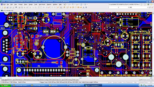
PCB Layout Design
PCB Layout Design is the process of transforming an electronic circuit schematic into a physical board design that can be manufactured and assembled. It involves strategically placing electronic components and creating conductive pathways (traces) to establish electrical connections. A well-designed PCB layout ensures optimal performance, reliability, and efficiency of the circuit. Designers focus on component placement, signal integrity, thermal management, and noise reduction. Modern PCB layout tools allow engineers to design multi-layer boards and prepare accurate files for fabrication, making the transition from concept to product smooth and efficient.
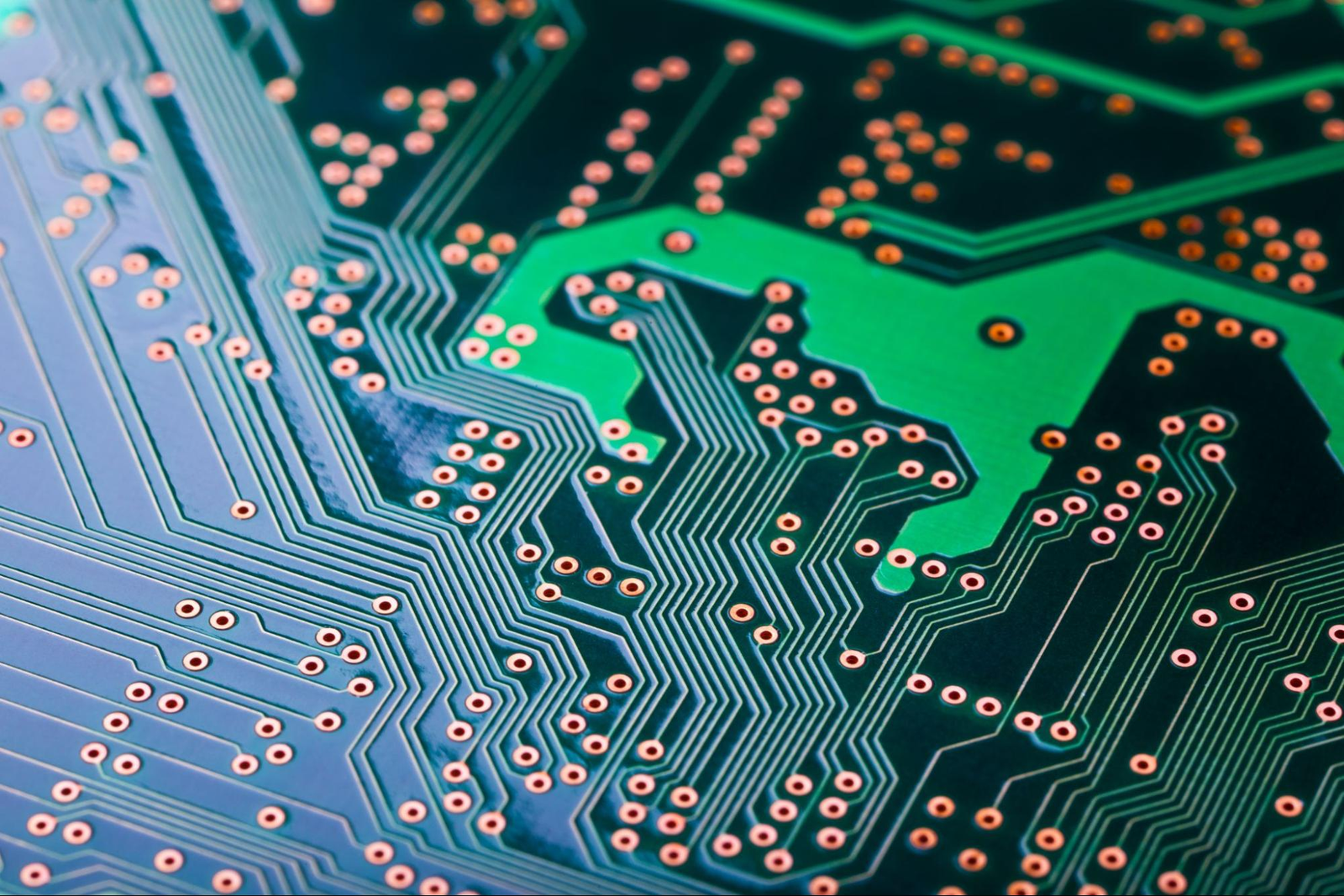
PCB Fabrication
PCB Fabrication is the process of converting a PCB design into a physical printed circuit board. It includes steps like printing the circuit pattern, etching unwanted copper, drilling holes, and applying protective layers. This process ensures durability and electrical reliability of the board. High-quality fabrication is essential for long-lasting and efficient electronic products. Advanced fabrication techniques support multi-layer and high-precision boards used in modern electronics.
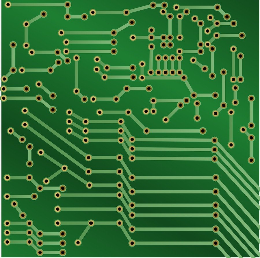
PCB Prototyping
PCB Prototyping is the process of creating a test version of a printed circuit board before mass production. It helps in verifying the design, identifying issues, and improving performance. Prototyping allows engineers to test real-world functionality, component placement, and system behavior, reducing the risk of costly errors. With rapid prototyping technologies, designs can be tested quickly, enabling faster product development and innovation.
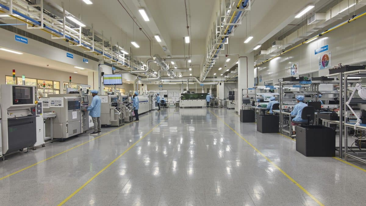
Electronics Manufacturing Services
Electronics Manufacturing Services (EMS) refers to a broad range of services provided by specialized companies that design, manufacture, test, distribute, and repair electronic components and assemblies for original equipment manufacturers (OEMs). These services allow companies to outsource their production processes, helping them reduce costs, improve efficiency, and focus on core activities like product design and marketing.